


Researchers at Michigan State University have developed a groundbreaking method to grow crystals with pinpoint accuracy, using a laser to guide their formation. This new technique could dramatically lower costs and improve the performance of electronic devices, from solar panels to advanced space telescopes.
The process, led by Elad Harel, uses a phenomenon known as plasmonic heating to essentially "draw" crystalline structures exactly where they are needed. This level of control overcomes major limitations of traditional crystal manufacturing, paving the way for more efficient and powerful technology.
Key Takeaways
- A new method uses a laser to heat a tiny gold nanoparticle, which then triggers crystal formation in a solution.
- This "plasmonic heating" allows scientists to precisely control the location, size, and shape of the crystals.
- The technique could replace less accurate and more wasteful traditional methods of crystal growth.
- Potential applications include more efficient LEDs, solar cells, medical imaging devices, and astronomical sensors.
A New Era of Crystal Fabrication
For decades, manufacturing crystals for electronics has been an imprecise science. Conventional methods often involve growing them in a solution and hoping they form in the right place, a process that can be haphazard and inefficient. This lack of control can lead to defects and wasted material.
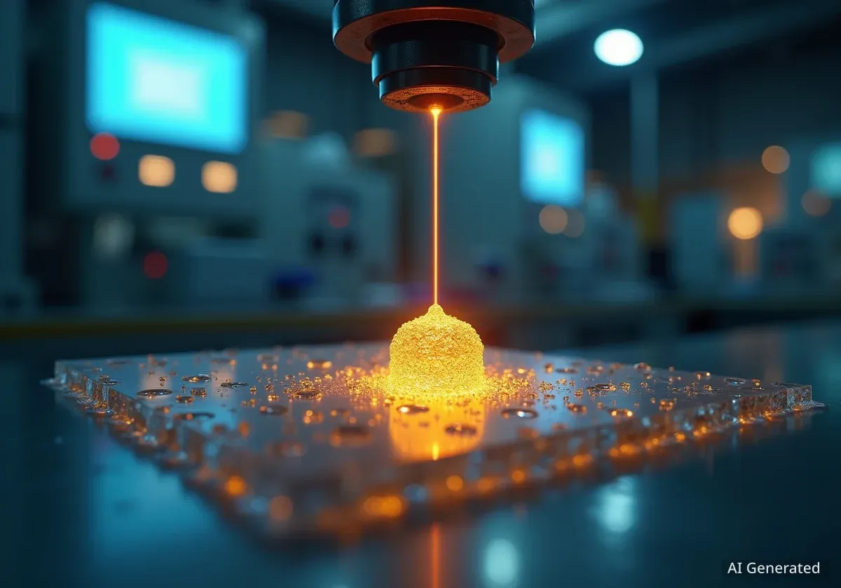
A team at Michigan State University has introduced a solution that offers unprecedented precision. By focusing a low-power laser on a single gold nanoparticle suspended in a chemical solution, they can generate a tiny, localized hot spot. This heat initiates the crystallization process, forming a solid crystal directly on a substrate.
"In a device, one may need a very small quantity of crystalline material placed at very specific locations," Elad Harel, who led the research team, explained. By moving the nanoparticle with the laser, his team can effectively draw lines and patterns, building crystalline structures from the ground up.
Microscopic Precision
The gold nanoparticles used in this process are incredibly small, measuring less than one-thousandth of the width of a human hair. This allows for the creation of intricate and microscopic crystalline circuits.
The Science of Plasmonic Heating
The core of this new technique is a physical effect called plasmonic heating. Gold nanoparticles are particularly effective at absorbing light at specific frequencies. When the laser hits the nanoparticle, it causes the electrons within the gold to oscillate rapidly, generating intense, localized heat.
"The reason we use gold nanoparticles is because they act as small heaters," Harel stated. "When a laser irradiates the particle at the right frequency, it causes the electrons in the gold to oscillate, which generates heat."
This heat is then transferred to the surrounding solution, in this case, a lead halide perovskite precursor. This specific material has an unusual property known as retrograde solubility, which is key to the process's success.
"What's special about these perovskites is that as the temperature increases the solubility decreases, which induces crystallization. Most materials do not exhibit this... typically as the temperature increases, the solubility increases."
This means that unlike sugar dissolving faster in hot water, perovskites solidify out of their solution when heated. The laser-heated nanoparticle creates the perfect conditions for a crystal to form exactly at its location.
Traditional vs. Modern Methods
Traditional crystal growth techniques, like vapor diffusion, rely on slowly changing the conditions of an entire solution to encourage crystals to precipitate out. This method offers little control over where crystals form or their final size, leading to inconsistencies in electronic components.
Wide-Ranging Applications and Future Steps
The ability to place high-quality crystals precisely where needed could transform numerous industries. Crystals are fundamental components in a vast array of modern technologies. The implications of this more efficient fabrication method are significant, potentially leading to cheaper and better-performing products.
Potential applications for this technology include:
- Solar Cells: Higher-performance perovskite solar panels with improved efficiency.
- LED Lighting: Brighter and more energy-efficient LEDs.
- Sensors and Detectors: More sensitive components for medical imaging, smoke alarms, and scientific instruments.
- Consumer Electronics: Advanced touchscreens and other optoelectronic devices.
- Space Exploration: Lower-cost, higher-performance sensors for astronomical instruments, such as those used on space telescopes.
The research team is already working to expand the technique's capabilities. Harel noted that his lab is exploring using multiple lasers at different wavelengths to draw more complex, multi-material patterns. The next phase involves fabricating and testing these drawn crystals in actual devices to validate their performance benefits.
While the initial success was with lead halide perovskites, Harel is optimistic about adapting the method for other materials. He suggests that the excited electrons in the gold nanoparticle might also participate directly in the chemical reaction, not just produce heat, which could allow the technique to be generalized for a wider range of crystals.
"This is a very simple method using low-cost lasers," Harel added. "It also saves enormously on the cost of fabrication since the crystal could be placed exactly where and when it is needed." The team's findings were published in the scientific journal ACS Nano.